Equations of a Solar Cell
Aditya N. Roy Choudhury 1![]()
1 Independent Researcher, Kolkata, India
|
|
|
ABSTRACT |
|
|
This paper
derives the algebraic expression of the short-circuit current of a solar cell
from first principles and explains the physics behind why a solar cell under
illumination supplies a current at zero applied voltage. Such simple
expressions have been absent previously from the solar cell literature. Apart
from the short-circuit current, this paper also gives simple theoretical
expressions for the open-circuit voltage and the efficiency of a solar cell.
All calculated current-voltage equations are corroborated with numerical
simulations. |
|||
|
Received 16 January 2025 Accepted 19 February 2025 Published 19 March 2025 Corresponding Author Aditya N.
Roy Choudhury, roychoudhury.aditya.2021@gmail.com DOI 10.29121/IJOEST.v9.i2.2025.675 Funding: This research
received no specific grant from any funding agency in the public, commercial,
or not-for-profit sectors. Copyright: © 2025 The
Author(s). This work is licensed under a Creative Commons
Attribution 4.0 International License. With the
license CC-BY, authors retain the copyright, allowing anyone to download,
reuse, re-print, modify, distribute, and/or copy their contribution. The work
must be properly attributed to its author.
|
|||
|
Keywords: Solar Cell,
Short-Circuit Current, Zero Applied Voltage |
|||
1. INTRODUCTION
Solar cells have been an active field of research in the last few decades Wilson et al. (2020) Lee & Ebong (2017); Kirchartz & Rau (2018). The conversion of light energy into electricity using semiconductors has both been scientifically satisfying and socially useful. In several households across the world, solar panels Nfaoui & El-Hami (2018); Durganjali et al. (2020), made of solar cells, have started supplying the much-needed electricity while the scientific study of the many different kinds of solar cells Wilson et al. (2020) has never been less intriguing.
A solar cell is a piece of a semiconductor device which, when illuminated, can supply an electrical current. In other words, it behaves like a battery when light shines on it. This has several fascinating applications mainly because unlike an electrical battery which functions due to the presence of chemicals inside it a solar cell does not have an expiry date. Light, from the sun, is also virtually an everlasting energy source.
The algebraic expression of the current the solar cell supplies at short-circuit, called the short-circuit current, is not found in research papers let alone its derivation from first principles. This paper fills this vacuum. This paper lists all the important parameters of the solar cell and expresses its various characteristics like the short-circuit current, open-circuit voltage and efficiency in terms of device parameters like the absorber thickness, illumination, doping densities and carrier mobilities which can be engineered during the fabrication of the device. In other words, this paper gives a first-hand thorough understanding of the working principles of the solar cell and also compares derived equations with results of numerical simulations and finds a reasonable agreement.
This paper considers a PIN silicon solar cell. Silicon solar cells have been the oldest and, still, the most used solar cells of all time Saga, T. (2010), Shah et al. (2004). PIN solar cells, unlike PN junction solar cells, has a separate absorber layer that absorbs the incident illumination Carlson & Wronski (1976); Pawlikiewicz & Guha (1990). We will see that understanding PIN solar cells is easier than PN junction solar cells as the in-built electric field in the absorber of a PIN solar cell is spatially uniform. It is also to be borne in mind that the thickness of the PIN absorber can be changed at will and this directly affects the value of the short-circuit current of the solar cell.
In what follows we first express the dark current of the solar cell. Then we derive the photocurrent of the solar cell from first principles. Next, we derive the total current. Expressions of open-circuit voltage and short-circuit current along with electrical efficiency are derived along the way. We also simulate the solar cell using ADEPT 2.1 Gray et al. (2015), a software that solves the Poisson Equations, the Continuity Equations and the Drift-Diffusion Equations simultaneously using a discrete mesh and a generalized Newton iteration method. We find reasonable agreement between the simulated results and the derived equations.
2. DARK CURRENT
To start, we consider a PIN structure of Silicon as in Figure 1 An I-type (intrinsic or undoped) silicon layer is considered sandwiched between a P-type and an N-type layer. The I-layer is also called the absorber.
Figure 1
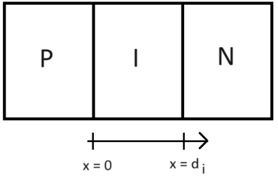
|
Figure
1 Schematic of the PIN
solar Cell Considered in this Work |
x is considered as the spatial variable. We will need x while solving for the photocurrent of the solar cell. The junction between the P-type and the I-type semiconductors is considered the origin. The thickness of the absorber is di.
First, we simulate the solar cell in the dark and find an expression of the dark current density JD in terms of the applied voltage V. This is called the dark J-V characteristics of the solar cell. For the simulation in ADEPT 2.1 we need to consider various material parameters like temperature, band gap, semiconductor layer thickness, carrier effective mass, carrier mobility, etc. which are tabulated in Table 1 Values for the band gap, electron affinity, dielectric constant, carrier mobilities and SRH recombination lifetimes in Silicon is taken from Ioffe website (semiconductor website). ADEPT requires the values of the conduction and valence band effective density of states (NC and NV) to compute the dark J-V curve which are calculated following Eqns. 1 and 2 Pierret (1996).
Table 1
|
Table 1 Parameters and their Values Chosen for Numerical Simulations in ADEPT 2.1 |
||
|
Parameter |
Symbol |
Value |
|
Temperature |
T |
300
K |
|
Material |
- |
Silicon |
|
Band
Gap |
- |
1.1
eV |
|
Electron
Affinity |
- |
4.05
eV |
|
Dielectric
Constant |
- |
11.7 |
|
Electron
or hole effective mass |
mn* or mp* |
1 x
(9.1 x 10-31 kg) |
|
Conduction
or valence band |
NC
or NV |
2.5
x 1019 / cc |
|
effective
Density of States |
||
|
Doping
density (P or N layer) |
NA
or ND |
1019
/ cc |
|
Doping
density (I layer) |
- |
0 |
|
Electron
or hole mobility (P or N layer) |
µn or µp |
100
cm2/ Vs |
|
Electron
mobility (I layer) |
- |
1000
cm2/ Vs |
|
Hole
mobility (I layer) |
- |
400
cm2/ Vs |
|
SRH
recombination lifetime |
τn or τp |
100
ns |
|
for electrons or holes |
||
|
(P or N layer) |
||
|
SRH
recombination lifetime |
- |
1 s |
|
for electrons or holes |
||
|
(I layer) |
||
|
Layer
thickness (P,I or N layer) |
di |
10
µm |
|
(for
I layer) |
||
|
Illumination
(I layer) |
- |
1
Sun (standard AM 1.5 G radiation) |
![]() (1)
(1)
![]() (2)
(2)
kB = 1.38 x 10⁻²³ J/K is the Boltzman constant, and ħ = (6.6 x 10⁻³⁴)/2π Js is the reduced Planck’s constant. The other symbols in Eqns. 1 and 2 are introduced in Table 1
In the dark the PIN solar cell behaves like a PIN diode. A PIN diode, as depicted in Figure 1, is like the PN diode but with an additional I-layer in between the doped layers. We know that the J-V characteristics of the PN junction follows the Shockley Ideal Diode Equation Pierret (1996). PIN diodes also follow Shockley Equation Roy Choudhury & Sarkar (2020). The derivation of the Shockley Equation thrives on solving the Continuity Equations in the quasi-neutral regions of the PN junction by equating the diffusion and recombination terms Pierret (1996). Such a derivation also holds for the PIN structure and therefore the Shockley Equation. The Shockley Equation is given in Eqn. 3.
![]() (3)
(3)
Here, JS is the saturation current density, and q = 1.6 x 10⁻¹⁹ C is the elementary electronic charge. The saturation current density is given by Eqn. 4 (R. F. Pierret, 1996).
![]() (4)
(4)
ni = 1010 / cc is the intrinsic carrier concentration of Silicon at room temperature [20]. The diffusion coefficient of the charge carrier (electron or hole) is related to the carrier’s mobility by Einstein’s relation (Eqn. 5) Pierret (1996). All other parameters in Eqn. 4 are introduced in Table 1.
![]() (5)
(5)
A point to note is that in this paper we do not consider any recombination of carriers within the absorber – neither in the numerical simulations nor in our calculations. A real solar cell will obviously have some recombination in its absorber, but the solar cell equations become comparatively long and complicated if recombination is accounted for. Just like we ignore the recombination in the depletion region of a PN junction while learning the PN junction and the Shockley Equation for the first time Pierret (1996) here we ignore absorber recombination while deriving the solar cell characteristics.
The result of the ADEPT 2.1 simulations is shown in Figure 2. We fit Eqn. 3 to the simulated curve and find that the dark current of the PIN solar cell obeys Shockley Equation. A comparison between the simulated results and the calculated results following the equations is given in Table 2.
Figure 2

|
Figure 2 (Color online) Numerically simulated and Fitted Dark Current Voltage Characteristics of the Solar Cell |
Table 2
|
Table 2 Simulated and Calculated Values of solar Cell Parameters |
|||
|
Parameter |
Symbol |
Simulated
Value |
Calculated
Value |
|
Saturation
Current Density |
JS |
5.6
x 10-14 A/cm2 |
1.6
x 10-14 A/cm2 |
|
Thermal
Voltage |
kBT/q |
26.3
mV |
25.9
mV |
|
Built-in
Voltage |
Vbi |
1.06
V |
1.08
V |
|
Generation
Rate in the I layer |
G |
1019
– 1021 /cc s |
2.7
x 1020 /cc s |
|
Open
Circuit Voltage |
VOC |
0.71
V |
0.74
V |
|
Short
Circuit Current Density |
JSC |
3.7
x 10-2 A/cm2 |
4.05
x 10-2 A/cm2 |
|
Voltage
at Maximum Power Point |
VMP |
0.63
V |
0.66
V |
|
Current
Density |
JMP |
3.6
x 10-2 A/cm2 |
3.9
x 10-2 A/cm2 |
|
at
Maximum Power Point |
|
|
|
|
Cell
Efficiency |
η |
22.70% |
25.60% |
|
Fill
Factor |
FF |
0.86 |
0.85 |
In Figure 2 the natural logarithm plot of the dark current density vs voltage follows a sub-linear behavior beyond 1 V. This occurs due to the series resistance Pierret (1996) of the PIN structure Roy Choudhury & Sarkar (2020). We do not analytically model this effect in our calculations because, as we will see in the later portions of this paper, the behavior of the dark current density in the linear region (up to 1 V) will be sufficient to explain the total current flowing through the solar cell.
3. PHOTOCURRENT
In the derivation of Eqn. 3, which is done in Pierret (1996), the Continuity Equations of the electron and hole concentrations in the dark are considered. Under illumination new electrons and holes are created inside the absorber and are transported to the P and N layers. These are the photocarriers, i.e. optically generated electrons and holes. The dynamics of these photocarriers are considered separately and they constitute what is called the photocurrent. The dark and the photo currents add to yield the total current of the solar cell.
We
start with the question: why a solar cell should supply a finite current at
zero applied voltage. The answer to this question lies in solving the
Continuity Equations and the Drift-Diffusion Equations under illumination which
we will do in this section. But qualitatively too the question can be answered.
The answer is this: like in a PN junction, in a PIN structure the charge
carrier depleted portions of the P and N layers give rise to an in-built
electric field. This electric field exists fully across the I-layer. At zero
applied voltage this built-in electric field gives rise to a finite current.
The built-in electric field can be expressed in terms of the built-in potential Vbi. The built-in potential is expressed in Eqn. 6 Pierret (1996).
![]() (6)
(6)
In presence of an applied voltage V, the total voltage across the PIN structure V’ is expressed by Eqn. 7.
![]() (7)
(7)
The total electric field E can now be expressed as
![]() (8)
(8)
Spatially this electric field is constant inside the I-layer. This occurs for a PIN structure unlike a PN junction where the electric field is triangularly shaped in space Pierret (1996).
![]() (9)
(9)
The Continuity Equations for holes in the absorber is given by Eqn. 10. Here p denotes the hole concentration in the absorber. t denotes time.
![]() (10)
(10)
Similarly, the Continuity Equation for electrons, where n denotes the electron concentration in the absorber, is given by Eqn. 11.
![]() (11)
(11)
Here G is the optical generation rate of the photocarriers in the absorber upon absorption of light. In reality, G is maximum at the semiconductor surface and decreases exponentially with distance inside the bulk Pierret (1996). This happens for each wavelength of light. The effect of all the wavelengths add up to yield the photocurrent. How much G falls with distance depends on the absorption coefficient of the semiconductor Pierret (1996). In ADEPT 2.1 simulations as well, when the absorber is illuminated, it is seen that G falls x. However, for a simple derivation of the photocurrent, in our calculations, we assume an average value of G throughout the absorber. This makes our calculated G spatially constant.
In Eqns. 12 – 16 the different terms of the Continuity Equations are expressed Pierret (1996). Here, Jp denotes the hole current and Jn denotes the electron current. ‘Drift’ and ‘diff’ in the subscripts mean the currents due the drift (electric field) and diffusion respectively.
![]() (12)
(12)
![]() (13)
(13)
![]() (14)
(14)
![]() (15)
(15)
![]() (16)
(16)
We are all set to solve for the photocurrent in the solar cell. However, before solving it one should be clear about the physics of the photocurrent. So, what really happens inside a solar cell Figure 1 when the absorber is illuminated at zero bias? The absorption of light in the I-layer generates new pairs of electrons and holes. Being inside a solar cell, these charge carriers feel two separate forces. First, they feel the built-in electric field. The P-layer has hole depleted acceptor ions towards the P-I interface. These are negatively charged. Similarly, the N-layer has electron depleted donor ions towards the I-N interface. These ions are positively charged. Thus, the built-in electric field is negative (directed towards the left of Figure 1. The photogenerated holes feel this field and drift to the left, while the photogenerated electrons drift to the right. This gives rise to a negative hole current and a negative electron current. Thus, the photocurrent is negative at zero bias. Apart from drift, diffusion also acts on the photogenerated carriers. Upon illumination, the absorber has all the generated photocarriers while the P and N layers have none (since the P and N layers are not fabricated in order to absorb light). Thus, the natural tendency of the photocarriers is to diffuse out of the absorber and to flow out to both the P and the N layers.
In what follows, we write the Continuity Equation for electrons (and holes) and solve the differential equation for the electronic (and hole) density. Then we derive the electron (and hole) currents and then the photocurrent. The Shockley Equation for the dark current (Eqn. 3) is derived in a similar way Pierret (1996). The only difference is that in the dark, the diffusion and recombination of charge carriers in the field-free P and N layers dominate the current, while under illumination the drift, diffusion and generation of charge carriers in the absorber makes the current flow.
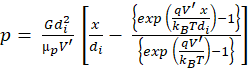
First, we solve for the hole concentration p. The drift current density of holes is expressed in Eqn. 17 Pierret (1996). Similarly, Eqn. 18 expresses the current density of holes due to diffusion Pierret (1996). Eqn. 19 expresses the total hole current density Pierret (1996).
![]() (17)
(17)
![]() (18)
(18)
![]() (19)
(19)
Now, from Eqns. 10, 12, 13, 14, 17, 18 and 19 we have Eqn. 20.
![]() (20)
(20)
![]() (21)
(21)
Eqn. 20 is a second order, linear differential equation which has an analytical solution as shown in Eqn. 21, where Cp1 and Cp2 are constants of integration.
Cp1 and Cp2 can be solved following two boundary conditions expressed in Eqns. 22 and 23. The holes considered here are photogenerated, and since absorption in the P and N layers is zero the hole concentrations at the boundaries of the absorber are also zero.
![]() (22)
(22)
![]() (23)
(23)
The constants of integration can be thus expressed in Eqns. 24 and 25.
![]() (24)
(24)
![]() (25)
(25)
The hole concentration in the absorber can therefore be finally derived as in Eqn. 26.
 (26)
(26)
Following Eqns. 26, 17, 18 and 19 the hole current density Jp can be expressed as in Eqn. 27.
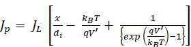 (27)
(27)
![]() (28)
(28)
The electronic concentration in the absorber n can be similarly solved following Eqns. 11, 12, 15, 16, 29, 30 and 31.
![]() (29)
(29)
![]() (30)
(30)
![]() (31)
(31)
The differential equation and its solution are given in Eqns. 32 and 33.
![]() (32)
(32)
 (33)
(33)
The total electronic current density is expressed in Eqn. 34.
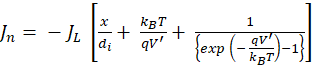 (34)
(34)
Finally, the photocurrent density Jph can be expressed, as in Eqn. 35, by summing the electron and the hole current densities.
![]() (35)
(35)
From. Eqns. 27, 28, 34 and 35 the expression of the solar cell’s photocurrent is obtained in Eqn. 36.
![]() (36)
(36)
The short-circuit current is the photocurrent at zero applied bias. In Eqn. 36, the short-circuit current density JSC can be obtained by putting V = 0. JSC is expressed in Eqn. 37.
![]() (37)
(37)
The expression of Eqn. 37 and the derivation of Eqn. 36 from the Continuity Equations are the central results of this paper. The constant JL is expressed in Eqn. 28. Such a simple expression of the short-circuit current density is required to understand the physics of solar cells, can be widely useful to the solar cell community, and was missing from the solar cell literature. To top it all, Eqn. 37 and its simple derivation can also be taught in undergraduate courses where solar cells are to be introduced to students. In most cases, JSC is close to JL but not equal. In other words, the order of magnitude of JSC and JL are the same. The term in the square brackets in Eqn. 37 provides a correction to the JSC ≈ JL approximation. The JSC ≈ JL approximation is a bad one and should not be used.
To check how well our calculated photocurrent tallies with a simulated curve, we simulate the photocurrent in ADEPT 2.1. The absorber is illuminated with 1 Sun of light, as mentioned in Table 1. Figure 3 show the simulated and the calculated photocurrent densities. We see that the calculations match the simulations reasonably.
Figure 3

|
Figure 3 (Color online) Simulated and Calculated Photocurrent Densities of the PIN solar cell |
4. TOTAL CURRENT AND SOLAR CELL EFFICIENCY
The total current density J of the solar cell can be expressed by summing the dark current density JD and the photocurrent density Jph, as in Eqn. 38.
![]() (38)
(38)
This current is bias dependent, starts at a finite negative value at zero volts, and approaches zero at a finite voltage less than Vbi (which is usually less than or close to 1 V).Figure 4 shows the total current densities of our solar cell – both simulated and the calculated J-V curves. Table 2 shows both the simulated and the calculated values of the short-circuit current density. It can be seen that the maximum error, when the calculations are compared with the simulations, is within 10%.
Figure 4

|
Figure 4 (Color online) The Total Current Densities of the Solar Cell – Both Simulated and Calculated |
For calculating the total current density Eqn. 39 is considered. It is to be noted that Eqn. 39 is true only near V = 0. However, for all practical purposes Eqn. 39 holds because the photocurrent stays nearly constant at JSC at low voltages (i.e. near V = 0) and drops to zero at V = Vbi. But at voltages lower than Vbi the dark current starts gaining magnitude over the photocurrent making the contribution of the photocurrent in the total current negligible. The voltage beyond which the dark current becomes greater than the photocurrent in magnitude is the open-circuit voltage VOC. VOC < Vbi.
![]() (39)
(39)
The total current becomes zero at the open-circuit voltage VOC. Like JSC, VOC is an important parameter of a solar cell. At zero bias the magnitudes of the dark current density and the photocurrent density (i.e. the short-circuit current density) becomes equal which suggests Eqn. 40. A modulus sign is used wherever necessary from now on because JSC < 0.
![]() (40)
(40)
Following Eqn. 40, the expression of VOC is expressed in Eqn. 41.
![]() (41)
(41)
The product of the total current density of the solar cell and the applied voltage yields the output power dissipated per unit cell area A. This power per unit area PA is expressed in Eqn. 42.
![]() (42)
(42)
When plotted vs applied bias, PA shows a maximum at V = VMP. The current density at this point is JMP. This is known as the maximum power point and is used to calculate the efficiency of a solar cell.
![]() (43)
(43)
By multiplying J to V and differentiating the JV product with respect to V and then equating the derivative at VMP to zero, we arrive at an expression for the voltage at the maximum power point as shown in Eqn. 44.
![]() (44)
(44)
Eqn. 44 leads to an explicit expression of VMP in terms of the Lambert W function. It is expressed in Eqn. 45.
![]() (45)
(45)
Eqn. 46 gives the expression for the total current density at the maximum power point.
![]() (46)
(46)
Figure 5 shows the comparison between the simulated and the calculated PA vs V curves.
The solar cell efficiency is given by Eqn. 47. The factor of 103 in the denominator denotes the input power per unit area of 1000 W/ m2 under 1 Sun illumination. The Fill Factor, another important solar cell parameter, is expressed in Eqn. 48.
![]() (47)
(47)
![]() (48)
(48)
Figure 5

|
Figure 5 (Colour online) Simulated and calculated curves of power per unit cell area vs applied bias |
Table 2 compares the simulated and the calculated values of VOC, η and FF. We see that in all cases the calculated values are quite close to the simulated ones.
5. CONCLUSION
This paper gives a simple derivation of the short-circuit current of a solar cell. Such an algebraic expression of the short-circuit current was missing from the solar cell literature.
In summary, this paper gives theoretical expressions, derived from first principles, for the bias dependent dark current density (Eqns. 3 and 4) [6], photocurrent density (Eqns. 36, 28, 7 and 6), total current density (Eqns. 38 and 39), as well as the open-circuit voltage (Eqn. 41), short-circuit current density (Eqn. 37), efficiency (Eqns. 47, 45 and 46) and fill factor (Eqn. 48) of a solar cell. All calculated equations match reasonably well with results of numerical simulations computed in software.
CONFLICT OF INTERESTS
None.
ACKNOWLEDGMENTS
None.
REFERENCES
Carlson, D. E., & Wronski, C. R. (1976). Amorphous Silicon Solar Cell. Applied Physics Letters, 28, 671-673. https://doi.org/10.1063/1.88617
Durganjali, C. S., Bethanabhotla, S., Kasina, S., & Radhika, D. S. (2020). Recent Developments and Future Advancements in Solar Panels Technology. Journal of Physics: Conference Series, 1495, 012018. https://doi.org/10.1088/1742-6596/1495/1/012018
Gray, J., Wang, X., Chavali, R. V. K., Sun, X., Kanti, A., & Wilcox, J. R. (2015). ADEPT 2.1. Retrieved from https://nanohub.org/resources/adeptnpt
Kirchartz, T., & Rau, U. (2018). What makes a Good Solar Cell? Advanced Energy Materials, 8, 1703385. https://doi.org/10.1002/aenm.201703385
Lee, T. D., & Ebong, A. U. (2017). A Review of thin-film Solar Cell Technologies and Challenges. Renewable and Sustainable Energy Reviews, 70, 1286-1297. https://doi.org/10.1016/j.rser.2016.12.028
Nfaoui, M., & El-Hami, K. (2018). Extracting the Maximum Energy from Solar Panels. Energy Reports, 4, 536-545. https://doi.org/10.1016/j.egyr.2018.08.002
Pawlikiewicz, A. H., & Guha, S. (1990). Numerical Modeling of an Amorphous-Silicon-Based P-I-N Solar Cell. IEEE Transactions on Electron Devices, 37, 403-409. https://doi.org/10.1109/16.47719
Pierret, R. F. (1996). Semiconductor device fundamentals. Addison-Wesley Publishing Company.
Roy Choudhury, A. N., & Sarkar, S. K. (2020). On the Linearity and Parabolicity of the PIN dark IV: The Effect of Series Resistance. 2020 5th IEEE International Conference on Emerging Electronics (ICEE), IEEE, 1-4. https://doi.org/10.1109/ICEE51202.2020.9356880
Saga, T. (2010). Advances in Crystalline Silicon solar Cell Technology for Industrial Mass Production. NPG Asia Materials, 2, 96-102. https://doi.org/10.1038/asiamat.2010.82
Semiconductor Website. (n.d.). Silicon Material Properties. Retrieved from https://www.ioffe.ru/SVA/NSM/Semicond/Si/index.html
Shah, A. V., Schade, H., Vanecek, M., Meier, J., Vallat-Sauvain, E., Wyrsch, N., Kroll, U., Droz, C., & Bailat, J. (2004). Thin-film sIlicon Solar Cell Technology. Progress in Photovoltaics, 12, 113-142. https://doi.org/10.1002/pip.524
Wilson, G. M., Al-Jassim, M., Metzger, W. K., Glunz, S. W., Verlinden, P., Xiong, G., Mansfield, L. M., Stanbery, B. J., Zhu, K., & Yan, Y. (2020). The 2020 Photovoltaic Technologies Roadmap. Journal of Physics D: Applied Physics, 53, 493001. https://doi.org/10.1088/1361-6463/ab9c6a
 This work is licensed under a: Creative Commons Attribution 4.0 International License
© Granthaalayah 2014-2025. All Rights Reserved.